The Silent Contender in Clean Tech: How Kesterite Cells Are Reshaping the Photovoltaic Horizon
What if the primary constraint holding back global clean energy expansion isn’t sunlight, but the critical minerals needed to harness it? Today, the world relies heavily on silicon wafers and specialized thin films to power the green transition. Yet, traditional solar panel manufacturing consumes vast amounts of silver, while alternative technologies depend on scarce or toxic elements like tellurium, indium, and cadmium.
As global demand for solar panels accelerates, energy scientists face a pressing question: can we build a photovoltaic technology that is non-toxic, structurally stable, and crafted entirely from cheap, widely available elements?
The answer lies in kesterite cells—an extraordinary class of thin-film photovoltaics that replaces rare minerals with copper, zinc, tin, and sulfur or selenium. By combining environmental safety with immense raw material availability, this emerging semiconductor technology represents a vital step forward in the evolution of clean energy.
What Are Kesterite Cells?
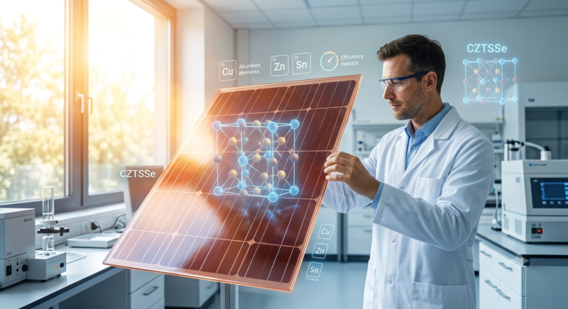
To understand why kesterite cells are generating such intense interest in materials science, one must look at the structural formula of their absorber layer. Commonly abbreviated as CZTSSe, kesterite is a quaternary compound composed of copper (Cu), zinc (Zn), tin (Sn), sulfur (S), and selenium (Se).
Unlike traditional silicon panels that require thick, energy-intensive wafers, kesterite cells belong to the family of high-absorption thin-film solar cells. Because kesterite possesses a direct optical bandgap and an exceptionally high absorption coefficient, a layer just a few micrometers thick can absorb nearly all incoming visible sunlight.
Historically, thin-film photovoltaics relied on materials like copper indium gallium selenide (CIGS) or cadmium telluride (CdTe). While effective, CIGS depends on indium and gallium—elements plagued by severe supply chain volatility—and CdTe contains toxic cadmium. By contrast, kesterite cells deliberately swap out these rare, restricted substances for abundant, non-toxic alternatives without forfeiting the fundamental physics of direct light absorption.
The Chemical Blueprint: Unleashing Earth-Abundant Materials
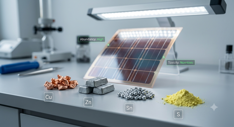
The defining breakthrough of kesterite technology is its total reliance on Earth-abundant materials. In sustainable engineering, a material’s practical viability is governed by its crustal concentration and geographic distribution.
Copper (Cu): Widely distributed globally, providing excellent electrical conductivity.
Zinc (Zn): An inexpensive, industrial metal that replaces rare indium.
Tin (Sn): A ubiquitous element that eliminates the need for expensive gallium.
Sulfur (S) & Selenium (Se): Naturally occurring non-metals that allow precise tuning of the semiconductor bandgap.
By synthesizing light-absorbing layers exclusively from Earth-abundant materials, manufacturers can insulate themselves against price spikes and geopolitical bottlenecks. This mineral security makes kesterite cells an ideal candidate for gigawatt-scale production lines needed for deep decarbonization.
How Kesterite Absorbs Light and Generates Electricity
The fundamental mechanics of kesterite cells follow the core principles of direct solar energy conversion. When incoming photons strike the light-absorbing CZTSSe layer, their energy excites electrons across the bandgap, creating mobile electron-hole pairs.
Once photogenerated carriers are created, internal electrical fields at the heterojunction interface separate them instantly:
Photon Absorption: Photons with energy matching or exceeding the 1.0–1.5 eV bandgap are absorbed within the top micrometer of the kesterite layer.
Carrier Generation: Electron-hole pairs form rapidly due to the semiconductor’s high absorption coefficient.
Interfacial Charge Separation: The internal electric field between the p-type kesterite layer and an n-type buffer layer (such as zinc oxide or cadmium sulfide) drives electrons toward the front contact and holes toward the back contact.
Current Extraction: The extracted charges travel through external circuitry, delivering usable electricity.
This direct path for solar energy conversion avoids the complex multi-step thermalization losses common in indirect-bandgap semiconductors, allowing extremely thin layers to perform heavy lifting.
Overcoming the Voltage Deficit: Pushing Power Conversion Efficiency Higher
Despite their ideal environmental credentials, kesterite cells have historically lagged behind CIGS and silicon in raw performance. The primary obstacle has been a phenomenon known as the “open-circuit voltage deficit,” caused by intrinsic cation disorder—where copper and zinc atoms swap positions in the crystal lattice—creating point defects and electron recombination centers.
However, recent breakthroughs in material passivation and defect control are transforming the landscape. Advanced annealing processes and molecular doping are dramatically reducing atomic disorder, propelling the laboratory power conversion efficiency of kesterite devices to new record highs.
By mitigating deep-level traps and optimizing heterojunction band alignment, world-class research institutes have pushed the certified power conversion efficiency of laboratory-scale kesterite cells past 13%, with theoretical limits extending beyond 30%. These steady gains demonstrate that kesterite is rapidly closing the performance gap with commercial thin films.
The Durability Advantage: Stability in Extreme Environments
While emerging solar materials like perovskites have captured headlines for rapid efficiency leaps, they face a known vulnerability: moisture and thermal degradation. Under prolonged exposure to ultraviolet light, heat, and ambient humidity, unpassivated perovskite layers can deteriorate rapidly.
Here, kesterite cells possess an inherent structural edge. Built upon robust inorganic mineral crystal lattices, kesterite absorbers display remarkable chemical resilience. Field tests demonstrate that kesterite cells maintain stable power output across months of continuous operation under high thermal stress and direct solar exposure without catastrophic performance degradation.
This structural ruggedness makes them particularly compelling for deployment in desert environments and high-humidity tropical zones where ambient conditions quickly degrade fragile organic or hybrid solar components.
Applications: Where Will Kesterite Cells Excel?
The unique physical properties of kesterite cells open up diverse application pathways that extend beyond conventional rooftop panel setups:
Building-Integrated Photovoltaics (BIPV): Because kesterite layers are extremely thin and semitransparent when applied to glass, they can be embedded directly into architectural windows, facades, and skylights.
Flexible Portable Electronics: Deposited on lightweight foil or polymer substrates, flexible kesterite cells can power wearable devices, sensors, and off-grid outdoors equipment.
Tandem Solar Architecture: Thanks to its tunable bandgap, wide-bandgap kesterite can serve as a top cell stacked above traditional silicon bottom cells, boosting overall panel yield without adding toxic materials.
This versatility positions kesterite as a key player across the entire spectrum of modern thin-film solar cells.
Sustainable Manufacturing and Lower Environmental Footprints
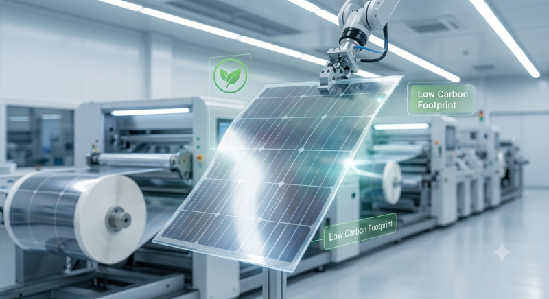
Evaluating clean energy technologies requires analyzing their total lifecycle, from raw material extraction to end-of-life recycling. Traditional silicon panel manufacturing demands high-temperature refining furnaces operating above 1,500°C, resulting in a noticeable embodied carbon footprint during initial production.
In contrast, thin-film solar cells using kesterite absorbers can be fabricated via low-temperature solution processing, spray pyrolysis, or electrodeposition. These gentle chemical synthesis routes dramatically reduce energy consumption during manufacturing.
Furthermore, because kesterite cells are synthesized entirely from non-toxic Earth-abundant materials, end-of-life recycling and disposal protocols are straightforward. The absence of heavy metals like lead or cadmium eliminates toxicity risks during decommission, simplifying environmental compliance and protecting surrounding ecosystems.
Scaling Up: What Lies Ahead for Commercialization?
To move from laboratory successes to global gigawatt manufacturing, the solar industry is actively resolving scale-up challenges. Depositing uniform, defect-free kesterite thin films across large surface areas requires ultra-precise atmospheric control during chemical vapor synthesis.
Fortunately, existing industrial equipment designed for manufacturing CIGS thin-film solar cells can be re-tooled for kesterite production with minimal capital expenditure. As processing methods refine, the combination of cheap raw inputs and low-energy synthesis will drive down the cost per watt of solar energy conversion.
As researchers continue passivating bulk defects and refining heterojunction interfaces, the practical power conversion efficiency of commercial kesterite modules will reach thresholds needed for commercial deployment, offering the world a truly sustainable photovoltaic alternative.
Frequently Asked Questions (FAQ)
What are kesterite cells?
Kesterite cells are thin-film photovoltaic devices that use a light-absorbing semiconductor layer made of copper, zinc, tin, and sulfur or selenium (CZTSSe). They are designed to deliver reliable solar energy conversion without using rare or toxic elements.
Why are Earth-abundant materials critical for next-generation solar energy?
Relying on Earth-abundant materials ensures that solar panel manufacturing can scale to terawatt levels without facing resource scarcity, supply chain disruptions, or steep material cost increases associated with rare metals like indium or tellurium.
How does the power conversion efficiency of kesterite compare to silicon?
Commercial silicon panels currently operate at 20% to 23% efficiency, whereas laboratory kesterite cells have surpassed 13% certified power conversion efficiency. While kesterite is still maturing, its theoretical efficiency limit exceeds 30%, giving it substantial upside as manufacturing methods improve.
Are kesterite cells toxic or difficult to recycle?
No. Unlike older thin-film technologies containing cadmium or newer hybrid devices containing lead, kesterite cells are constructed from non-toxic elements. This clean composition significantly lowers environmental risks and simplifies recycling procedures at the end of the panel’s operational lifespan.

Trusted by 50000+ Customers
Anya Green Energy is a leading solar company and Solar Energy service provider established in 2013. We are recognized by startup India and customer best choice award 2022.
Our Achievements :
Recognized by Startup India.
Purvanchal’s first solar company to operate exclusively with solar products.
Certified by well-known institutions such as MSME, IndiaMart, and Just Dial and many more.
Winner of the Best Customer Choice Award 2022.
Over 50,000 happy customers across India.